| Issue |
EPJ Appl. Metamat.
Volume 6, 2019
Metamaterials Research and Development in Korea
|
|
|---|---|---|
| Article Number | 12 | |
| Number of page(s) | 15 | |
| DOI | https://doi.org/10.1051/epjam/2019010 | |
| Published online | 22 February 2019 | |
https://doi.org/10.1051/epjam/2019010
Review
Recent progress in angle-insensitive narrowband and broadband metamaterial absorbers
School of Electrical and Electronics Engineering, Chung-Ang University, Seoul, Republic of Korea
* e-mail: This email address is being protected from spambots. You need JavaScript enabled to view it.
Received:
20
September
2018
Accepted:
3
February
2019
Published online: 22 February 2019
Abstract
Recent progress in angle-insensitive narrowband and broadband metamaterial absorbers is presented herein. Initially, a few narrowband structures are described along with their absorption mechanisms. A bandwidth-enhanced absorber, conceptually derived from the existing narrowband geometry, is also discussed. Finally, several broadband absorbers having wide absorption bandwidths across different microwave frequency ranges are illustrated. The reported structures are primarily designed to exhibit high angularly stable responses suitable for practical applications. Furthermore, their geometries are fourfold symmetric, thereby displaying polarization-independent characteristics. Experimental verifications of the designed absorbers have been confirmed under normal and oblique incidences. The angle insensitivity, polarization independence, flexible absorption bandwidths (from narrowband to broadband), and commercial feasibility of the reported structures might establish them as potential candidates for manifold absorber applications.
Key words: Metamaterials / electromagnetic absorbers / angle insensitivity / broadband absorbers
© S. Ghosh et al., published by EDP Sciences, 2019
 This is an Open Access article distributed under the terms of the Creative Commons Attribution License (http://creativecommons.org/licenses/by/4.0), which permits unrestricted use, distribution, and reproduction in any medium, provided the original work is properly cited.
1 Introduction
Electromagnetic (EM) metamaterials (MMs) are artificial composite structures engineered to exhibit unique features not available in natural materials [1,2]. Owing to their properties in the subwavelength scale, MMs can manipulate the effective permittivity and permeability parameters in a wide range, from very small values to extremely large values, and even negative values in some cases [3–5]. Therefore, MMs have been exploited in various applications, e.g., super lens [6], antennas [7], filters [8], and cloaking [9]. The MM absorber is another breakthrough in this domain [10] that can be used as a potential alternative to conventional absorbers owing to their near-unity absorption properties, ultrathin thickness, simple manufacturing procedures, and increasing effectiveness.
Numerous absorber applications are available across civil and defense sectors. The reduction in the radar cross section is a crucial application [11], where the target is coated with microwave absorbers to reduce the detectability of the object by radar. In household applications, various electrical instruments need to be shielded to avoid any EM interference [12]. Other typical applications include solar cells [13], photodetectors [14], sensors [15], thermal emitters [16], and bolometers [17]. Some of these applications require narrowband absorptions (bolometers, sensors), whereas others use broadband absorbers covering wide bandwidths (stealth technology). As MM absorbers are built on large periodic arrays, their absorption responses depend on the incident as well as on the polarization angles of the incident EM wave [18]. However, practical applications require such kind of absorber structures whose performances will remain constant over any incident and/or polarization angle. Therefore, microwave absorbers having angular and polarization angle stability characteristics are urgently required in the research fraternity.
Herein, a recent progress in angle- and polarization-independent MM absorbers is discussed in detail. In the initial sections, various narrowband structures are described along with their absorption mechanisms. Later, broadband absorbers are presented based on the resistive concept. All the geometries are fourfold symmetric in nature, thereby resulting in polarization-insensitive characteristics. The structures are further designed to exhibit higher angularly stable responses as compared to the existing absorbers. Finally, a summary of the absorber structures is presented in the tabular format, along with the possible advancements in the near future.
2 Absorption mechanism of metamaterial absorbers
An MM absorber is typically built on a commercially available dielectric substrate, on which periodic arrays of conductive patterns are imprinted. The top layer geometry exerts an effective inductance and an effective capacitance, whereas the loss is attributed to the substrate. Depending on the pattern geometry and dielectric properties, single or multiple narrowband/broadband absorption responses can be obtained from the structure.
In 2008, Landy et al. [10] experimentally demonstrated a narrowband MM absorber, based on the combination of an electric ring resonator and a cut wire. The two asymmetrical patterns are periodically etched on the opposite sides of an FR4 substrate. When the plane EM wave is incident on the geometry, the design is excited such that both electric and magnetic resonances are generated. This simultaneously reduces the reflection as well as transmission coefficients of the structure and exhibits a narrowband absorption at 11.65 GHz. The proposed technique has several significant advantages over the conventional microwave absorbers such as thin profile, ease of fabrication, commercial availability, and practical effectiveness.
Henceforth, researchers have been actively investigating various types of MM absorbers that exhibit diverse characteristics. With the evolution in design principles, the rear side of the absorber structures has been shielded with complete metal plates [19,20]. This has led to the elimination of transmission responses from the geometries, and the subsequent absorbers are primarily emphasized in reducing the reflection coefficient only from the designs.
The absorptivity of a structure can be characterized as follows: A = 1 – |S 11|2 – |S 21|2, where S 11 and S 21 are the reflection and transmission coefficients, respectively. Because the MM absorbers are of subwavelength-scaled geometries, other phenomena such as scattering and diffraction are too insignificant to be considered. With the complete ground plane, the transmission is zero; thus, the equation above is reduced to A = 1 – |S 11|2. Thus, the absorptivity of a structure can be maximized through minimizing the reflection from the geometry.
The reflection coefficient at the interface is related to the input impedance of the structure according to the following equation [21]: (1)where Z
in and Z
0 are the input impedance of the structure and free space impedance, respectively. It is clearly observed that the reflection coefficient becomes zero when Z
in = Z
0, i.e., when the structure is perfectly impedance matched to the free space. In summary, a structure will exhibit near-unity absorption if its input impedance is matched to the free space impedance (and no transmission at the back). Narrowband or broadband absorptions occur based on the nature of impedance matching of the geometry: matching at one frequency causes narrowband absorption, whereas matching over a wide frequency range results in broadband absorption.
(1)where Z
in and Z
0 are the input impedance of the structure and free space impedance, respectively. It is clearly observed that the reflection coefficient becomes zero when Z
in = Z
0, i.e., when the structure is perfectly impedance matched to the free space. In summary, a structure will exhibit near-unity absorption if its input impedance is matched to the free space impedance (and no transmission at the back). Narrowband or broadband absorptions occur based on the nature of impedance matching of the geometry: matching at one frequency causes narrowband absorption, whereas matching over a wide frequency range results in broadband absorption.
However, the equation above is valid for normal incidences only. Under an oblique incidence, the reflection coefficient equation changes for perpendicular polarization (Γ⊥) and parallel polarization (Γ||), as given by [21]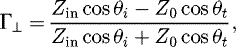 (2)
(2)
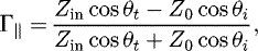 (3)where θi
and θt
are the incident and transmission angles, respectively. Therefore, a structure must be carefully designed such that the proposed geometry will satisfy both equations (2) and (3) with different incident angles, to obtain an angle-insensitive MM absorber. Although a polarization-independent absorber can be easily constructed by arranging horizontally and vertically symmetric unit cells in a periodic array, it is challenging to simultaneously satisfy equations (2) and (3) (and subsequently realize angle insensitivity). Some of the reported structures exhibit stable absorption behaviors up to a certain angle of incidence, and those geometries are generally termed as angularly stable absorber structures. In the following sections, a compressive study of such angularly stable as well as polarization-insensitive MM absorbers are described in detail.
(3)where θi
and θt
are the incident and transmission angles, respectively. Therefore, a structure must be carefully designed such that the proposed geometry will satisfy both equations (2) and (3) with different incident angles, to obtain an angle-insensitive MM absorber. Although a polarization-independent absorber can be easily constructed by arranging horizontally and vertically symmetric unit cells in a periodic array, it is challenging to simultaneously satisfy equations (2) and (3) (and subsequently realize angle insensitivity). Some of the reported structures exhibit stable absorption behaviors up to a certain angle of incidence, and those geometries are generally termed as angularly stable absorber structures. In the following sections, a compressive study of such angularly stable as well as polarization-insensitive MM absorbers are described in detail.
3 Narrowband metamaterial absorbers
Narrowband MM absorber structures offer single or multiple absorption peaks, whose resonances are very sharp, and offer limited bandwidths. These structures are primarily used in different types of sensors, imaging instruments, bolometers, and other related applications, where sharp resonances are critical. Such absorbers are typically constructed based on the top metallic pattern resonances, whereas the loss is primarily generated from the dielectric substrates [22,23]. The top geometry, made from conductive patches, offers small ohmic losses insufficient for good absorption. Therefore, a lossy dielectric is often preferred in a narrowband absorber structure (unlike other microwave devices) [24].
To achieve narrowband absorption responses, numerous geometries have been explored over the last decade, e.g., square loop, square slot, Jerusalem cross, circular patch, and circular slot [25–30]. However, most of these existing topologies display poor absorption performances under oblique incidence, in particular beyond a certain angle of incidence. Therefore, different strategies have been implemented by various researchers to realize angle-independent MM absorbers. Some of the promising geometries are described in the following sections.
3.1 Four circular sector-based patch geometry
Lee et al. have developed a narrowband absorber structure, where the top metallic pattern comprises a center square patch connected with four circular sectors around the patch [31]. The sectors are separated from one another through symmetric slots to realize the capacitive effect. The overall pattern was printed on a substrate, whose rear side was completely metal laminated. FR4 (relative permittivity (εr ) of 4.4 and dielectric loss tangent (tan δ) of 0.02) was used as the dielectric in the structure. The top and bottom metal patches were made of copper having a conductivity (σ) of 5.8 × 10⁷ S/m and a thickness of 0.035 mm. The physical dimensions along with the unit cell geometry of the proposed absorber are presented in Figure 1a.
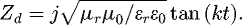
The top metallic patch exerts an equivalent inductance (L) and capacitance (C) to the geometry, whereas the grounded dielectric, acting as a short-circuited transmission line, provides an imaginary impedance. An equivalent resistance (R) is obtained owing to the finite conductivity of the metal. Therefore, the input impedance of the structure can be expressed as [32,33] (4)
(4)
 (5)
Here, εr
and μr
are the real parts of the relative permittivity and permeability of the dielectric, respectively.
(5)
Here, εr
and μr
are the real parts of the relative permittivity and permeability of the dielectric, respectively. 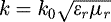 is the wavenumber of the incident EM wave. Therefore, by controlling the geometric parameters of the topology, the input impedance of the structure (Z
in) can be perfectly matched to the free space impedance (Z
0) at a particular frequency. This results in minimal reflection coefficient, whereas the transmission coefficient is also zero (due to the presence of ground plane). Then, the incident EM wave gets completely absorbed in the geometry through the ohmic loss (in the top metallic layer) and the dielectric loss (in the intermediate substrate).
is the wavenumber of the incident EM wave. Therefore, by controlling the geometric parameters of the topology, the input impedance of the structure (Z
in) can be perfectly matched to the free space impedance (Z
0) at a particular frequency. This results in minimal reflection coefficient, whereas the transmission coefficient is also zero (due to the presence of ground plane). Then, the incident EM wave gets completely absorbed in the geometry through the ohmic loss (in the top metallic layer) and the dielectric loss (in the intermediate substrate).
Because the primary focus is to design an angularly stable MM absorber, other criteria must be satisfied along with the impedance matching condition [34]. An angle-insensitive absorber structure not only retains the absorptivity magnitude with higher incident angles, the absorption frequency also remains constant. Although some of the earlier geometries (e.g., Jerusalem cross) result in high absorption under oblique incidence, their absorption frequencies become deviated at higher incident angles [31]. Thus, the sole purpose of designing the angle-insensitive absorber has become futile. In the proposed geometry, both the absorptivity and absorption frequency have been maintained relatively constant to obtain an angularly stable absorber structure.
While investigating the proposed structure for various incident angles, it is found that the deviation in the absorption response under oblique incidence can be significantly reduced by optimizing some of the physical dimensions of the geometry. A theoretical term, i.e., angle sensitivity (SA
), has been defined as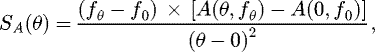 (6)where f
θ and f
0 are the resonant frequencies at the angles of incidence θ° and 0° (i.e., normal incidence), respectively. A(θ, fθ
) is the absorption magnitude corresponding to an absorption frequency fθ
at θ° incident angle. A(0, f
0) is the absorptivity under normal incidence, where the absorption occurs at f
0 frequency. As shown in equation (6), the smaller the value of angle sensitivity (SA
), the more angle insensitive the structure.
(6)where f
θ and f
0 are the resonant frequencies at the angles of incidence θ° and 0° (i.e., normal incidence), respectively. A(θ, fθ
) is the absorption magnitude corresponding to an absorption frequency fθ
at θ° incident angle. A(0, f
0) is the absorptivity under normal incidence, where the absorption occurs at f
0 frequency. As shown in equation (6), the smaller the value of angle sensitivity (SA
), the more angle insensitive the structure.
Figure 1c shows a histogram plotting of SA for different values of the parameter α, where α is the inner angle at each of the circular sectors. As SA exhibits the lowest value corresponding to α = 90°, the structure is optimized for this set of dimensions, and the simulated scattering coefficients are presented in Figure 1b. The unit cell geometry of the proposed structure is simulated in a finite-element-method-based EM solver ANSYS high-frequency structure simulator (HFSS) software, using periodic boundary conditions. Floquet port excitations are utilized in the simulation setup to mimic the infinite periodic structure into a unit cell configuration. The transmission coefficient is zero owing to metal backing, whereas a narrowband reflection dip is observed at 10.44 GHz. This corresponds to a near-unity absorption at 10.44 GHz having an absorptivity of 91%, as depicted in Figure 1b.
The response above has been analyzed under normal incidence. The structure must be studied for different polarizations as well as incident angles to confirm its polarization- and angle-insensitive characteristics. During simulation, the structure exhibits almost similar absorption responses for all the polarization angles under normal incidence, as observed in Figure 2a. In the simulation setup, the incident wave propagation direction remains constant, whereas the incident electric and magnetic field vector directions are varied with the angle of polarization (ϕ). Physically, an incident electric field vector of any arbitrary polarization can be divided into two components: vertical and horizontal. Owing to the fourfold symmetric geometry, the design exhibits identical behaviors for both modes, thereby providing polarization-independent characteristic.
The proposed geometry has also been studied under oblique incidence. Two different cases may occur under oblique incidence: in one condition, the incident electric field direction remains constant, whereas the magnetic field and wave propagation directions are rotated with the incident angle (θ). This is known as perpendicular polarization or transverse electric (TE) polarization. The modified reflection coefficient term during TE polarization is expressed in equation (2). On the contrary, the incident magnetic field direction remains the same, and the electric field and wave propagation vector directions are varied with the incident angle in the other case. This phenomenon is known as parallel polarization or transverse magnetic (TM) polarization. Equation (3) shows the reflection coefficient formula corresponding to this mode. During simulation, phase delay between the master and slave boundary is varied to change the incident angle of the EM wave, whereas the selection of the polarization (TE/TM) can be regulated by the floquet port excitation. Figures 2b and 2c display the simulated absorption responses of the proposed structure under TE and TM polarizations, respectively. As observed, the geometry exhibits an absorptivity higher than 90%, and the variation in the absorption frequency becomes less than 0.96% for incident angles up to 70°. Therefore, the design can be considered as an angularly stable MM absorber, as claimed by the authors.
To demonstrate the proposed absorber, a prototype was fabricated on a commercial FR4 substrate using printed circuit board (PCB) technology and measured in the anechoic chamber using the free space technique. The sample exhibited good agreement between the measured and simulated responses under normal as well as oblique incidences.
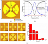 |
Fig. 1 (a) Proposed unit cell geometry along with its physical dimensions: a = 6 mm, b = 2.2 mm, c = 0.8 mm, g = 0.5 mm, w = 2.3 mm, α = 90°, and thickness (t) = 0.6 mm. (b) Simulated reflection coefficient, transmission coefficient, and absorptivity of the optimized structure. (c) Angle-sensitivity (SA ) of the topology for different values of the inner angle (α) and corresponding geometries [31]. |
 |
Fig. 2 Simulated absorptivity of the proposed absorber (a) for different polarization angle under normal incidence, and for different incident angles under (b) TE polarization, and (c) TM polarization [31]. |
3.2 Four circular sector-based slot geometry
Nguyen et al. have later modified the topology above and proposed a narrowband absorber based on its complement geometry (with some modifications in the physical dimensions) [35]. Figure 3a illustrates the unit cell configuration, where the top metallic pattern is based on a slot geometry, and the substrate is backed by a ground plane. The geometry, owing to inductive and capacitive effects, results in a narrowband absorption at 10.05 GHz with 91.48% absorptivity. The structure has also been studied for different values of the internal angle (α) and revealed that the geometry achieves the least angle sensitivity (SA ) performance at α = 85°. Figure 3b shows that the simulated absorptivity of the optimized structure under TE polarization exceeds 90% absorptivity in all the cases until θ = 70°. However, the proposed design suffers from two disadvantages: (i) an additional absorption peak is observed at approximately 11 GHz during larger incident angles owing to the higher order resonance; (ii) the absorption frequency shift is considerably large during TM polarization (not shown here). In an aperture-based geometry, effective inductance and capacitance occur in parallel combination, and their contributions significantly get deviated with the incident electric field [36]. This subsequently shifts the absorption frequency under TM-polarized incident EM wave. Therefore, it can be concluded that the previous patch-based geometry provides better angular stability response compared to this slot topology. Hence, the subsequent absorber structures discussed herein are based on the patch configuration only.
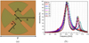 |
Fig. 3 (a) Proposed unit cell geometry along with its physical dimensions: P = 9.1 mm, R = 4.3 mm, W = 0.9 mm, D = 2.6 mm, L = 2.96 mm, thickness = 0.8 mm, and α = 85°. (b) Simulated absorptivity of the proposed structure for different incident angles under TE mode [35]. |
3.3 Eight circular sector-based patch geometry
From the earlier observations, the patch geometry was shown to provide a better angularly stable response. Therefore, the concept has been further extended by increasing the number of patches in the circular sector topology. Nguyen and Lim have designed another narrowband absorber structure, whose unit cell geometry comprises eight circular sector patterns on the top of a grounded dielectric [37]. The properties of the substrate and metal are similar, as mentioned in the previous geometries. The proposed absorber design is presented in Figures 4a and 4b.
Owing to the larger number of circular sectors, the topology exhibits an improved angular response compared to the previous two absorbers [38]. Here, the absorption frequency is observed at 9.26 GHz with 96% absorptivity at normal incidence. The structure, while simulated under oblique incidence, displays an absorptivity higher than 90% until 70° incident angle, and the absorption frequency variation is limited to within 0.7%, for both TE and TM polarizations. Figures 4b and 4c depict the simulated responses of the proposed structure for different incident angles. Our experimental validation has also confirmed the proposed absorber concept.
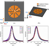 |
Fig. 4 Proposed unit cell geometry along with its physical dimensions: P = 10 mm, R 1 = 0.81 mm, R 2 = 3.2 mm, L = 2.4 mm, W = 0.3 mm, and thickness = 0.8 mm. (a) Top view. (b) Perspective view. Simulated absorptivity of the proposed absorber for different incident angles under (b) TE mode and (c) TM mode [37]. |
3.4 Via-array-based geometry
In addition to the circular sector-based geometry, other techniques can be used to realize angle-insensitive MM absorbers. Lim et al. have presented a via-array-based structure that exhibits an improved angular response compared to its counterpart [39]. The proposed design consists of a split ring cross-resonator arranged periodically on a grounded dielectric substrate. The properties of the dielectric and the metal are similar, as previously reported. Figure 5 illustrates the proposed structure along with its physical dimensions.
The geometry, with and without metallic vias, exhibits narrowband absorption at 11.31 and 11.35 GHz, respectively, at 0° incident angle. Thus, no significant difference is observed with the inclusion of the via array, particularly at normal incidence. However, when the incident angle is gradually increased, both the absorptivity and absorption frequency deviate from that of the normal incidence response for the via-less structure, as observed in Figure 6a. On the contrary, the absorption frequency remains almost constant under oblique incidence after the inclusion of the via array, as depicted in Figure 6b. As the incidence angle gets wider, the coupling between adjacent split ring cross-resonators becomes higher. The angle insensitivity is achieved by reduction of coupling level due to the proposed via array. The proposed geometry was also fabricated using PCB technique, measured under normal and oblique incidences, and was found to exhibit good agreement between the simulated and measured responses.
 |
Fig. 5 Unit cell geometry of the proposed absorber structure: (a) top view and (b) perspective view. The optimized physical dimensions are as follows: Lu = 8 mm, Lc = 6.8 mm, Ro = 3.3 mm, Ri = 2.4 mm, Rc = 2.05 mm, Wr = 0.9 mm, Wc = 2.9 mm, Gc = 0.3 mm, Rv = 0.2 mm, Go = 0.75 mm, Gv = 0.5 mm, and Hu = 0.35 mm [39]. |
 |
Fig. 6 Simulated absorptivities of the proposed structure under TE polarization: (a) without via array and (b) with via array [39]. |
3.5 Multilayer geometry
Multilayer technology can also be used to produce MM absorbers [40,41]. Yoo et al. have proposed an MM absorber based on a multilayer geometry to reduce the electrical size of the unit cell, as well as to improve the angular response of the structure [42]. Figure 7 depicts the unit cell configuration of the structure, which consists of three layers: a conductive ring in the top layer, a split ring cross-resonator in the middle layer, and inductive meander lines in the bottom layer. Metallic vias were used to connect the middle and bottom layer patterns, which lower the absorption frequency owing to the increase in the capacitance value. The overall geometry is backed by a metal ground to eliminate transmissions through the structure. A significant improvement in the angular response of the geometry, owing to this metal–insulator–metal capacitance, has also been experimentally confirmed, as shown in Figures 7c and 7d. The structure resulted in an absorptivity higher than 90% until 40° incident angle for TE polarization, whereas almost perfect absorptivity (above 95%) was observed until 60° during TM polarization.
 |
Fig. 7 Unit cell geometry of the proposed absorber: (a) top view and (b) perspective view. The geometric dimensions are a = 0.6 mm, b = 0.9 mm, c = 0.1 mm, d = 0.2 mm, e = 0.1 mm, f = 0.4 mm, g = 1.2 mm, h = 0.4 mm, i = 2.5 mm, j = 2.7 mm, k = 0.06 mm, l = 0.3 mm, and m = 0.2 mm. Measured absorptivity of the proposed absorber at different incident angles under (c) TE polarization (d) TM polarization [42]. |
4 Broadband metamaterial absorbers
Because MM absorbers are produced from the resonance mechanism, the absorption bandwidths are typically narrow. These narrowband absorbers, although suitable for limited applications, cannot be utilized in other operations, e.g., stealth technology [43] and wideband shielding [44]. Therefore, broadband absorbers covering several microwave bands (C, X) are in great demand. Before realizing broadband absorbers, researchers have attempted to increase the absorption bandwidths originating primarily from the existing narrowband absorbers [45–48]. This produces a number of bandwidth-enhanced geometries, whose bandwidths are considerably larger than those of the narrowband absorbers, but smaller than those of the broadband structures.
4.1 Bandwidth-enhanced absorber using hybrid geometry
One of the conventional techniques to realize a bandwidth-enhanced absorber is to use a hybrid unit cell geometry [49,50]. Two different sets of resonating structures (having different absorption frequencies) are embedded in a single unit cell that exhibit two absorption peaks. By properly optimizing the design parameters of the structure, these two frequencies can be brought closer to realize a bandwidth-enhanced absorption.
A few bandwidth-enhanced MM absorbers have been presented based on the technique above; however, most of these structures exhibit poor angular responses under oblique incidence. Because the circular sector-based geometry has resulted in an improved absorption response at higher incident angles, Nguyen and Lim have implemented the concept in achieving a bandwidth-enhanced absorber with angle insensitivity [51]. The proposed geometry comprises a periodic arrangement of four circular sector metallic patches imprinted on a grounded dielectric substrate, as shown in Figure 8a. In the unit cell, the first and fourth patterns (marked “A”) are identical, whereas the second and third patches (marked “B”) are similar. These two variations in the circular sector geometries are different from each other by a few geometric dimensions. Owing to the small difference in the parameters, these two sets of resonating structures give rise to two distinct absorption peaks that are close to each other. By properly optimizing the dimensions, these peaks have been brought together, and resulted in a bandwidth-enhanced absorber. The absorption responses of the individual metallic patches (“A” and “B”) along with the combined response are illustrated in Figure 8b. The “A” and “B” patches exhibit near-unity absorption at 10.38 and 10.55 GHz, respectively, whereas the hybrid unit cell results in an enhanced absorption bandwidth from 10.25 to 10.65 GHz. Thus, the fractional bandwidth increases to 7.66% from 1.94%, as obtained from the single peak geometry [31].
As the unit cell topology is fourfold symmetric, the structure provides a constant absorption bandwidth and frequency for all the polarization angles. The fabricated prototype was also measured under different polarization angles, and the polarization-insensitive characteristics were experimentally demonstrated. Figures 8c and 8d depict the simulated absorption behaviors of the geometry at different incident angles under TE and TM modes, respectively, and it is found that the absorption magnitude exceeds 91% at approximately 10.41 GHz at an angle of incidence up to 70° in both the polarizations. The measured responses display an absorptivity above 90% at the center frequency until 70° incident angle; thereafter, the absorption responses gradually reduce. The proposed structure has also been compared with earlier reported bandwidth-enhanced absorbers, and was found to exhibit larger absorption bandwidths, in particular at higher incident angles (60° and 70°) for TE and TM polarizations.
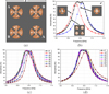 |
Fig. 8 (a) Top view of the proposed bandwidth-enhanced MM absorber. The geometric dimensions are as follows: P = 17.6 mm, R 1 = 2.8 mm, R 2 = 2.89 mm, W 1 = 1.22 mm, W 2 = 1.6 mm, G 1 = 0.7 mm, G 2 = 0.7 mm, and thickness = 0.8 mm. (b) Simulated absorptivity of the proposed structure along with its individual counterparts under normal incidence. Simulated absorptivity of the proposed structure at different incident angles under (c) TE polarization and (d) TM polarization [51]. |
4.2 Broadband absorber using four circular sector geometry
Although the technique above exhibits a bandwidth-enhanced MM absorber, the absorption bandwidth is limited to a few hundred megahertz only. However, most of the practical applications demand an absorption bandwidth on the order of a few gigahertz, along with an absorptivity level above 90%. Therefore, new absorption mechanisms are to be implemented for realizing such wideband absorbers.
Nguyen and Lim have therefore incorporated the circuit analog (CA) concept in the circular sector geometry to increase the absorption bandwidth [52]. A CA-based absorber is an effective solution to resolve the narrow bandwidth problem, where broadband absorption is obtained by appropriately depositing resistive and conductive patterns on a dielectric substrate [53]. This periodic resistive–conductive pattern of the CA absorber can be realized by mounting lumped resistors across the gaps present in the metallic patterns printed on the dielectric substrates [54–57].
The proposed design is composed of four circular patch sectors connected at the center through a square patch, and the overall geometry is patterned on a grounded dielectric substrate in a periodic array. The properties of the dielectric and metal are similar, as mentioned in the previous geometries. To increase the absorption bandwidth, four lumped resistors are symmetrically mounted across the slots between the circular sectors, as illustrated in Figure 9a. The lumped resistors, owing to a high ohmic loss, absorb the incident EM wave over a large frequency range and exhibit broadband absorption (above 90%) from 7.1 to 13.5 GHz under normal incidence.
Because the geometry is fourfold symmetric and the lumped components are mounted symmetrically, the structure provides identical absorption responses for all the polarization angles. Therefore, the topology can be considered as polarization independent. The proposed structure has also been studied under oblique incidence, as depicted in Figures 9c and 9d. In the TE mode, the absorption magnitude slowly reduces with higher incident angles. Nevertheless, the broadband absorptivity of above 90% is still achieved between 7 and 12.2 GHz up to 50° incident angle.
However, the absorption characteristics change differently under TM polarization. Instead of a gradual reduction in the absorption bandwidth, a sharp decrease occurred in the absorptivity at approximately 10 GHz with higher incident angles, and this effectively divides the absorption bandwidth into two spectra. This results in a reduced absorption from 7.1 to 9.4 GHz at 50° incident angle. Therefore, the proposed structure, although exhibiting polarization-insensitive broadband absorption under normal incidence, cannot provide good angularly stable characteristics, in particular during TM polarization.
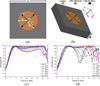 |
Fig. 9 Proposed broadband absorber with four circular sector geometry: (a) top view and (b) side view. The optimized geometric dimensions are the following: P = 14 mm, W = 3.45 mm, L = 2.485 mm, a = 0.65 mm, b = 3.4 mm, c = 0.5 mm, h = 3.4 mm, and R = 150 Ω. Simulated absorptivity of the proposed structure at different incident angles under (c) TE polarization and (d) TM polarization [52]. |
4.3 Broadband absorber using eight circular sector geometry
The disadvantage (of having poor absorption performance under TM mode) in the previous structure has been improved in the subsequent geometry, as presented by Nguyen and Lim [58]. The proposed geometry consists of an eight-resistive arm arranged circularly on a grounded dielectric substrate. Lumped resistors of 100 Ω are mounted across the gaps in each of the arms to realize wideband absorption. With the increase in the number of arms, the topology becomes eightfold symmetric, unlike the fourfold symmetry in the previous geometry. This results in an improved angular response of the structure. Figures 10a and 10b illustrate the top view and perspective view, respectively, of the unit cell geometry of the proposed absorber.
When the geometry without the lumped resistors is studied, two narrowband absorption frequencies are obtained at 8.89 and 13.20 GHz, as observed in Figure 10c. These sharp resonances are generated owing to the similar absorption mechanisms described in the previous section. However, with the inclusion of the lumped components, the incident EM wave gets absorbed over a wide frequency range and exhibits an absorptivity greater than 90% in the range of 8.2–13.4 GHz. This corresponds to a fractional bandwidth of 48.15%, as shown in Figure 10d. The equivalent circuit models for both geometries have also been investigated and were found to agree well with the simulated responses, as depicted in the figures.
The proposed geometry, owing to its eightfold symmetry, results in a polarization-insensitive behavior, as presented in Figure 11a. The structure is studied for different polarization angles under normal incidence, and the absorptivity remains nearly constant in the range of 8–13.6 GHz for all polarization angles. Furthermore, the design is analyzed under oblique incidence, and revealed that the absorptivity gradually decreases with higher incident angles. The structure can still maintain a 90% absorptivity in the range of 8.5–11.7 GHz up to 60° incident angle during TE polarization. In the TM mode, the absorptivity reduces at a higher rate with the incident angle and manages to exhibit an absorption bandwidth over the frequency range of 10.5–12.3 GHz at the angle of incidence 60°. Figures 11b and 11c illustrate the absorption spectra of the proposed geometry for different incident angles under TE and TM polarizations, respectively. It is clearly observed that the proposed design exhibits improved angular stable performances compared to the previous geometry, owing to the increase in the number of resistive arms in the topology.
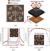 |
Fig. 10 Unit cell geometry of the proposed broadband absorber: (a) top view and (b) perspective view. The final geometric dimensions are P = 15.5 mm, R = 7.3 mm, R 1 = 6.1 mm, R 2 = 1 mm, L 1 = 2.5 mm, L 2 = 2 mm, w = 0.6 mm, e = 0.6 mm, g = 1.7 mm, and d = 3 mm. Comparison of the absorptivities obtained from numerical simulation using Ansys HFSS and circuit level simulation: (c) structure without resistors and (d) structure with resistors [58]. |
 |
Fig. 11 Simulated absorption spectra of the proposed broadband absorber (a) for different polarization angles under normal incidence, and for different incident angles under (b) TE polarization and (c) TM polarization [58]. |
5 Conclusions
We herein presented a compressive study of the recently published narrowband and broadband MM absorbers. The structures described in this article were aimed to exhibit polarization-insensitive and angularly stable absorption responses, unlike most of the earlier reported MM absorbers. Initially, a few narrowband microwave absorbers were illustrated along with their absorption mechanisms. Subsequently, broadband absorbers were discussed in detail. The presented articles are summarized in Table 1 in terms of their absorption characteristic, thickness, polarization insensitivity, and angularly stable behaviors. Owing to their manifold advantages, these structures could be used as potential candidates for various types of absorber applications. The proposed geometries could also be explored to realize reconfigurable absorbers with multifunctional responses.
Summary of performances of presented MM absorbers.
Acknowledgments
This work was supported by the National Research Foundation of Korea (NRF) grant funded by the Korea government (MSIP) (No. 2017R1A2B3003856).
References
- C. Caloz, T. Itoh, Electromagnetic metamaterials, transmission line theory and microwave applications, 1st ed. (John Wiley & Sons, Inc., New York, 2006) [Google Scholar]
- N. Engheta, R.W. Ziolkowski, Metamaterials: physics and engineering explorations, 1st ed. (John Wiley & Sons, Inc., New York, 2006) [Google Scholar]
- J.B. Pendry, A.J. Holden, W.J. Stewart, I. Youngs, Extremely low frequency plasmons in metallic mesostructure, Phys. Rev. Lett. 76 , 4773 (1996) [CrossRef] [PubMed] [Google Scholar]
- J.B. Pendry, A.J. Holden, D.J. Robbins, W.J. Stewart, Magnetism from conductors and enhanced nonlinear phenomena, IEEE Trans. Microw. Theory Tech. 47 , 2075 (1999) [Google Scholar]
- D.R. Smith, W.J. Padilla, D.C. Vier, S.C. Nemat-Nasser, S. Schultz, Composite medium with simultaneously negative permeability and permittivity, Phys. Rev. Lett. 84 , 4184 (2000) [CrossRef] [PubMed] [Google Scholar]
- N. Fang, H. Lee, C. Sun, X. Zhang, Sub-diffraction-limited optical imaging with a silver superlens, Science 308 , 534 (2005) [CrossRef] [PubMed] [Google Scholar]
- Y. Dong, T. Itoh, Metamaterial-based antennas, Proc. IEEE 100 , 2271 (2012) [CrossRef] [Google Scholar]
- J. Bonache, I. Gil, J. Garcia-Garcia, F. Martin, Novel microstrip bandpass filters based on complementary split-ring resonators, IEEE Trans. Microw. Theory Tech. 54 , 265 (2006) [CrossRef] [Google Scholar]
- D. Schurig et al., Metamaterial electromagnetic cloak at microwave frequencies, Science 314 , 977 (2006) [CrossRef] [PubMed] [Google Scholar]
- N.I. Landy, S. Sajuyigbe, J.J. Mock, D.R. Smith, W.J. Padilla, Perfect metamaterial absorber, Phys. Rev. Lett. 100 , 207402 (2008) [CrossRef] [PubMed] [Google Scholar]
- A. Fallahi et al., Thin wideband radar absorbers, IEEE Trans. Antennas Propag. 58 , 4051 (2010) [CrossRef] [Google Scholar]
- H. Wakatsuchi, D.F. Sievenpiper, C. Christopoulos, Designing flexible and versatile metamaterial absorbers, IEEE Electromagn. Compat. Mag. 5 , 76 (2016) [CrossRef] [Google Scholar]
- J.-J. Greffet et al., Coherent emission of light by thermal sources, Nature 416 , 61 (2002) [CrossRef] [PubMed] [Google Scholar]
- J. Rosenberg, R.V. Shenoi, T.E. Vandervelde, S. Krishna, O. Painter, A multispectral and polarization-selective surface-plasmon resonant midinfrared detector, Appl. Phys. Lett. 95 , 161101 (2009) [CrossRef] [Google Scholar]
- N. Liu, M. Mesch, T. Weiss, M. Hentschel, H. Giessen, Infrared perfect absorber and its application as plasmonic sensor, Nano Lett. 10 , 2342 (2010) [CrossRef] [PubMed] [Google Scholar]
- M. Diem, T. Koschny, C.M. Soukoulis, Wide-angle perfect absorber/thermal emitter in the terahertz regime, Phys. Rev. B 79 , 033101 (2009) [CrossRef] [Google Scholar]
- P.L. Richards, Bolometers for infrared and millimeter waves, J. Appl. Phys. 76 , 1 (1994) [NASA ADS] [CrossRef] [Google Scholar]
- O. Luukkonen, F. Costa, C.R. Simovski, A. Monorchio, S.A. Tretyakov, A thin electromagnetic absorber for wide incidence angles and both polarizations, IEEE Trans. Antennas Propag. 57 , 3119 (2009) [CrossRef] [Google Scholar]
- H. Tao et al., A metamaterial absorber for the terahertz regime: design, fabrication and characterization, Opt. Exp. 16 , 7181 (2008) [Google Scholar]
- H. Li et al., Ultrathin multiband gigahertz metamaterial absorbers, J. Appl. Phys. 110 , 014909 (2011) [CrossRef] [Google Scholar]
- D.M. Pozar, Microwave engineering, 2nd ed. (John Wiley & Sons, Inc., New York, 2008) [Google Scholar]
- H.-X. Xu et al., Tripleband polarization-insensitive wide-angle ultra-miniature metamaterial transmission line absorber, Phys. Rev. B 86 , 205104 (2012) [CrossRef] [Google Scholar]
- C.G. Hu, X. Li, Q. Feng, X.N. Chen, X.G. Luo, Investigation on the role of the dielectric loss in metamaterial absorber, Opt. Exp. 18 , 6598 (2010) [Google Scholar]
- J.E. Raynolds, Ohmic loss in frequency-selective surfaces, J. Appl. Phys. 93 , 5346 (2003) [CrossRef] [Google Scholar]
- X. Shen et al., Polarization-independent wide-angle triple-band metamaterial absorber, Opt. Exp. 19 , 9401 (2011) [Google Scholar]
- L. Li, Y. Yang, C. Liang, A wide-angle polarization-insensitive ultra-thin metamaterial absorber with three resonant modes, J. Appl. Phys. 110 , 063702 (2011) [CrossRef] [Google Scholar]
- H. Zhai, C. Zhan, Z. Li, C. Liang, A triple-band ultrathin metamaterial absorber with wide-angle and polarization stability, IEEE Antennas Wireless Propag. 14 , 241 (2015) [CrossRef] [Google Scholar]
- J.W. Park et al., Multi-band metamaterial absorber based on the arrangement of donut-type resonators, Opt. Exp. 21 , 9691 (2013) [Google Scholar]
- S. Bhattacharyya, S. Ghosh, K.V. Srivastava, Equivalent circuit model of an ultra-thin polarization-independent triple band metamaterial absorber, AIP Adv. 4 , 097127 (2014) [CrossRef] [Google Scholar]
- Z. Mao et al., Multi-band polarization-insensitive metamaterial absorber based on Chinese ancient coin-shaped structures, J. Appl. Phys. 115 , 204505 (2014) [CrossRef] [Google Scholar]
- D. Lee, J.G. Hwang, D. Lim, T. Hara, S. Lim, Incident angle- and polarization-insensitive metamaterial absorber using circular sectors, Sci. Rep. 6 , 27155 (2016) [CrossRef] [Google Scholar]
- S. Ghosh, K.V. Srivastava, An equivalent circuit model of FSS-based metamaterial absorber using coupled line theory, IEEE Antennas Wireless Propag. Lett. 14 , 511 (2015) [CrossRef] [Google Scholar]
- F. Costa, A. Monorchio, G. Manara, Analysis and design of ultrathin electromagnetic absorbers comprising resistively loaded high impedance surfaces, IEEE Trans. Antennas Propag. 58 , 1551 (2010) [CrossRef] [Google Scholar]
- S.A. Tretyakov, S.I. Maslovski, Thin absorbing structure for all incidence angles based on the use of a high-impedance surface, Microw. Opt. Technol. Lett. 38 , 175 (2003) [CrossRef] [Google Scholar]
- T.T. Nguyen, D. Lee, H.K. Sung, S. Lim, Angle- and polarization-insensitive metamaterial absorber based on vertical and horizontal symmetric slotted sectors, Appl. Opt. 55 , 8301 (2016) [CrossRef] [Google Scholar]
- O. Luukkonen et al., Simple and accurate analytical model of planar grids and high-impedance surfaces comprising metal strips or patches, IEEE Trans. Antennas Propag. 56 , 1623 (2008) [CrossRef] [Google Scholar]
- T.T. Nguyen, S. Lim, Wide incidence angle-insensitive metamaterial absorber for both TE and TM polarization using eight-circular-sector, Sci. Rep. 7 , 3204 (2017) [CrossRef] [Google Scholar]
- B. Sanz-Izquierdo, E.A. Parker, Dual polarized reconfigurable frequency selective surfaces, IEEE Trans. Antennas Propag. 62 , 764 (2014) [CrossRef] [Google Scholar]
- D. Lim, D. Lee, S. Lim, Angle- and polarization-insensitive metamaterial absorber using via array, Sci. Rep. 6 , 39686 (2016) [CrossRef] [Google Scholar]
- Y. Cheng, Y. Nie, R. Gong, Metamaterial absorber and extending absorbance bandwidth based on multi-cross resonators, Appl. Phys. B 111 , 483 (2013) [CrossRef] [Google Scholar]
- S. Ghosh, S. Bhattacharyya, D. Chaurasiya, K.V. Srivastava, Polarisation-insensitive and wide-angle multi-layer metamaterial absorber with variable bandwidths, Electron. Lett. 51 , 1050 (2015) [CrossRef] [Google Scholar]
- M. Yoo, H.K. Kim, S. Lim, Angular- and polarization-insensitive metamaterial absorber using subwavelength unit cell in multilayer technology, IEEE Antennas Wireless Propag. Lett. 15 , 414 (2016) [CrossRef] [Google Scholar]
- W.F. Bahret, The beginnings of stealth technology, IEEE Trans. Aerosp. Elect. Syst. 29 , 1377 (1993) [CrossRef] [Google Scholar]
- S. Celozzi, R. Araneo, G. Lovat, Electromagnetic shielding, 1st ed. (John Wiley & Sons, Inc., New York, 2008) [CrossRef] [Google Scholar]
- J. Lee, S. Lim, Bandwidth-enhanced and polarization-insensitive metamaterial absorber using double resonance, Electron. Lett. 47 , 8 (2011) [CrossRef] [Google Scholar]
- H. Yang et al., Low RCS metamaterial absorber and extending bandwidth based on electromagnetic resonances, Prog. Electromagn. Res. M 33 , 31 (2013) [CrossRef] [Google Scholar]
- S. Bhattacharyya, S. Ghosh, D. Chaurasiya, K.V. Srivastava, Bandwidth-enhanced dual-band dual-layer polarization-independent ultra-thin metamaterial absorber, Appl. Phys. A 118 , 207 (2015) [CrossRef] [Google Scholar]
- J. Lee, M. Yoo, S. Lim, A study of ultra-thin single-layer frequency selective surface microwave absorbers with three different bandwidths using double resonance, IEEE Trans. Antennas Propag. 63 , 221 (2015) [CrossRef] [Google Scholar]
- S. Ghosh, S. Bhattacharyya, K.V. Srivastava, Bandwidth-enhancement of an ultrathin polarization insensitive metamaterial absorber, Microw. Opt. Technol. Lett. 56 , 350 (2014) [CrossRef] [Google Scholar]
- D. Kundu, A. Mohan, A. Chakraborty, Ultrathin polarization independent absorber with enhanced bandwidth by incorporating giusepe peano fractal in square ring, Microw. Opt. Technol. Lett. 57 , 1072 (2015) [CrossRef] [Google Scholar]
- T.T. Nguyen, S. Lim, Bandwidth-enhanced and wide-angle-of-incidence metamaterial absorber using a hybrid unit cell, Sci. Rep. 7 , 4814 (2017) [CrossRef] [Google Scholar]
- T.T. Nguyen, S. Lim, Angle- and polarization-insensitive broadband metamaterial absorber using resistive fan-shaped resonators, Appl. Phys. Lett. 112 , 021605 (2018) [CrossRef] [Google Scholar]
- B.A. Munk, Frequency selective surfaces: theory and design, 1st ed. (John Wiley & Sons, Inc., New York, 2000) [Google Scholar]
- Y. Shang, Z. Shen, S. Xiao, On the design of single-layer circuit analog absorber using double-square-loop array, IEEE Trans. Antennas Propag. 61 , 6022 (2013) [CrossRef] [Google Scholar]
- M. Yoo, S. Lim, Polarization-independent and ultrawideband metamaterial absorber using a hexagonal artificial impedance surface and a resistor-capacitor layer, IEEE Trans. Antennas Propag. 62 , 2652 (2014) [CrossRef] [Google Scholar]
- B.K. Kim, B. Lee, Design of metamaterial-inspired wideband absorber at X-Band adopting trumpet structures, KIEES J. Electromagn. Eng. Sci. 14 , 314 (2014) [CrossRef] [Google Scholar]
- S. Ghosh, S. Bhattacharyya, K.V. Srivastava, Design, characterisation and fabrication of a broadband polarisation-insensitive multi-layer circuit analogue absorber, IET Microw. Antennas Propag. 10 , 850 (2016) [CrossRef] [Google Scholar]
- T.T. Nguyen, S. Lim, Design of metamaterial absorber using eight-resistive-arm cell for simultaneous broadband and wide-incidence-angle absorption, Sci. Rep. 8 , 6633 (2018) [CrossRef] [Google Scholar]
Cite this article as: Saptarshi Ghosh, Toan Trung Nguyen, Sungjoon Lim, Recent progress in angle-insensitive narrowband and broadband metamaterial absorbers, EPJ Appl. Metamat. 6, 12 (2019)
All Tables
All Figures
|
Fig. 1 (a) Proposed unit cell geometry along with its physical dimensions: a = 6 mm, b = 2.2 mm, c = 0.8 mm, g = 0.5 mm, w = 2.3 mm, α = 90°, and thickness (t) = 0.6 mm. (b) Simulated reflection coefficient, transmission coefficient, and absorptivity of the optimized structure. (c) Angle-sensitivity (SA ) of the topology for different values of the inner angle (α) and corresponding geometries [31]. |
| In the text | |
|
Fig. 2 Simulated absorptivity of the proposed absorber (a) for different polarization angle under normal incidence, and for different incident angles under (b) TE polarization, and (c) TM polarization [31]. |
| In the text | |
|
Fig. 3 (a) Proposed unit cell geometry along with its physical dimensions: P = 9.1 mm, R = 4.3 mm, W = 0.9 mm, D = 2.6 mm, L = 2.96 mm, thickness = 0.8 mm, and α = 85°. (b) Simulated absorptivity of the proposed structure for different incident angles under TE mode [35]. |
| In the text | |
|
Fig. 4 Proposed unit cell geometry along with its physical dimensions: P = 10 mm, R 1 = 0.81 mm, R 2 = 3.2 mm, L = 2.4 mm, W = 0.3 mm, and thickness = 0.8 mm. (a) Top view. (b) Perspective view. Simulated absorptivity of the proposed absorber for different incident angles under (b) TE mode and (c) TM mode [37]. |
| In the text | |
|
Fig. 5 Unit cell geometry of the proposed absorber structure: (a) top view and (b) perspective view. The optimized physical dimensions are as follows: Lu = 8 mm, Lc = 6.8 mm, Ro = 3.3 mm, Ri = 2.4 mm, Rc = 2.05 mm, Wr = 0.9 mm, Wc = 2.9 mm, Gc = 0.3 mm, Rv = 0.2 mm, Go = 0.75 mm, Gv = 0.5 mm, and Hu = 0.35 mm [39]. |
| In the text | |
|
Fig. 6 Simulated absorptivities of the proposed structure under TE polarization: (a) without via array and (b) with via array [39]. |
| In the text | |
|
Fig. 7 Unit cell geometry of the proposed absorber: (a) top view and (b) perspective view. The geometric dimensions are a = 0.6 mm, b = 0.9 mm, c = 0.1 mm, d = 0.2 mm, e = 0.1 mm, f = 0.4 mm, g = 1.2 mm, h = 0.4 mm, i = 2.5 mm, j = 2.7 mm, k = 0.06 mm, l = 0.3 mm, and m = 0.2 mm. Measured absorptivity of the proposed absorber at different incident angles under (c) TE polarization (d) TM polarization [42]. |
| In the text | |
|
Fig. 8 (a) Top view of the proposed bandwidth-enhanced MM absorber. The geometric dimensions are as follows: P = 17.6 mm, R 1 = 2.8 mm, R 2 = 2.89 mm, W 1 = 1.22 mm, W 2 = 1.6 mm, G 1 = 0.7 mm, G 2 = 0.7 mm, and thickness = 0.8 mm. (b) Simulated absorptivity of the proposed structure along with its individual counterparts under normal incidence. Simulated absorptivity of the proposed structure at different incident angles under (c) TE polarization and (d) TM polarization [51]. |
| In the text | |
|
Fig. 9 Proposed broadband absorber with four circular sector geometry: (a) top view and (b) side view. The optimized geometric dimensions are the following: P = 14 mm, W = 3.45 mm, L = 2.485 mm, a = 0.65 mm, b = 3.4 mm, c = 0.5 mm, h = 3.4 mm, and R = 150 Ω. Simulated absorptivity of the proposed structure at different incident angles under (c) TE polarization and (d) TM polarization [52]. |
| In the text | |
|
Fig. 10 Unit cell geometry of the proposed broadband absorber: (a) top view and (b) perspective view. The final geometric dimensions are P = 15.5 mm, R = 7.3 mm, R 1 = 6.1 mm, R 2 = 1 mm, L 1 = 2.5 mm, L 2 = 2 mm, w = 0.6 mm, e = 0.6 mm, g = 1.7 mm, and d = 3 mm. Comparison of the absorptivities obtained from numerical simulation using Ansys HFSS and circuit level simulation: (c) structure without resistors and (d) structure with resistors [58]. |
| In the text | |
|
Fig. 11 Simulated absorption spectra of the proposed broadband absorber (a) for different polarization angles under normal incidence, and for different incident angles under (b) TE polarization and (c) TM polarization [58]. |
| In the text | |
Current usage metrics show cumulative count of Article Views (full-text article views including HTML views, PDF and ePub downloads, according to the available data) and Abstracts Views on Vision4Press platform.
Data correspond to usage on the plateform after 2015. The current usage metrics is available 48-96 hours after online publication and is updated daily on week days.
Initial download of the metrics may take a while.