| Issue |
EPJ Appl. Metamat.
Volume 13, 2026
|
|
|---|---|---|
| Article Number | 13 | |
| Number of page(s) | 14 | |
| DOI | https://doi.org/10.1051/epjam/2025017 | |
| Published online | 13 May 2026 | |
https://doi.org/10.1051/epjam/2025017
Original article
Inverse design of multiwavelength multifocal metalens based on the tandem neural networks
School of Artifical Intelligence Science and Technology, University of Shanghai for Science and Technology, Shanghai 200093, PR China
* e-mail: This email address is being protected from spambots. You need JavaScript enabled to view it.
Received:
1
October
2025
Accepted:
9
December
2025
Published online: 13 May 2026
Abstract
Metalenses, as the typical diffractive optical device, provide a platform for the research of the optical imaging and light field modulation, and have received massive attraction. However, the traditional complex design process relies on the numerical solutions of Maxwell’s equations and requires high computational and time resources. In recent years, the inverse design based on the nerual networks provides an effective method for the design of the diffractive optical devices, and improve the the design freedom and efficiency. In this paper, an inverse design method for multifocal metalens based on the tandem neural network is proposed, and achieves efficient forward prediction of the phases, and the design of structural parameters. Based on this network, a single-focus metalens designed with the target focal length of 9 μm has been achieved with the design error controlled below 2.8%. On the foundation, this method can also be used to realize the design of the multifocal metalens. The dual-wavelength metalens is first designed to realize the recognition of specific wavelength p and multifocal imaging, and then expanded to four wavelengths. The study has potential applications in the field of optical communication, imaging, detection, etc.
Key words: Inverse design / multifocal metalens / tandem neural networks
© Y. Song et al., Published by EDP Sciences, 2026
 This is an Open Access article distributed under the terms of the Creative Commons Attribution License (https://creativecommons.org/licenses/by/4.0), which permits unrestricted use, distribution, and reproduction in any medium, provided the original work is properly cited.
1 Introduction
Metasurfaces, which are the two-dimensional subwavelength planar arrays of the artificial materials have a wide range of applications in the field of nanophotonics, like metalenses [1,2], optical filters [3], holography [4,5]. Comparing to the traditional lenses, metalenses have widely studied for the potentials of the characteristics, like ultrathin, miniaturization, and high focusing efficiency [6–8]. They can flexibly manipulate the polarization, phase and amplitude states of wavefronts by changing the geometry parameters and the orientation of the unit nanostructures, and provide a reliable platform for the realization of diffractive optical devices and unusual functions, including achromatic metalenses [9,10], multifocal metalenses [11–13], polarization‐insensitive metalenses [14], etc. Multifocal metalenses, which can focus the incident beam to several positions in the longitudinal or transverse direction, have special applications in the biomedical, and imaging system [15]. In addition, the muliwavelength metalenses can enhance and recognize the number of operating wavelengths, paving the way for the optical communication, and optical integration [16]. The muliwavelength multifocal metalenses are expected to have unique impacts in the fields of multi-imaging, polarization detection, manipulation of the states of nanostructures.
In the traditional design process, the design and optimization rely on the abundant physical knowledge and extensive experience, and require large complex numerical simulations, solving Maxwell’s equations, to sweep and select the ideal structural parameters, which satisfy the specific optical responses [17,18]. However, the process costs massive time and computational resources, limiting the efficiencies and flexibility. With the rapid development of the computer performance and artificial intelligence, inverse design, using mathematical tools to solve physical problems, has been introduced into the design process [19,20]. It begins from the desired optical responses, and then achieves the corresponding geometry parameters by using computational methods, such as Genetic Algorithm (GA) [21], Topology Optimization (TO) [22], particle swarm optimization (PSO) [23], and deep learning (DL) [24,25]. As a data-driven approach based on neural networks (NNs), DL can discover and learn the nonintuitive relationships among unknown large datasets composed of geometry parameters and optical responses [26]. In recent years, some progress has been made in the studies, using DL to optimize inverse designs. An et al. combined the conditional generative adversarial network (CGAN) with the Wasserstein Generative Adversarial Networks (WGAN), which stabilized the network and solved the complexity of parallel processing by introducing earth-mover distance [27]. The inverse design neural network was used to design the meta-atoms of the free-form all-dielectric multifunctional metalenses, like the bifocal metalens, the polarization-multiplexed metalens as well as multi-channel or bandwidth-controllable metasurface [28–31]. Luo et al. designed the two-layer multifocal diffractive device based on the adaptive deep diffractive neural networks (a-D2NNs), which can achieve back propagation through diffraction layers without the need of the datasets [32]. The efficiency of the device exceeded 50% at both wavelengths of 632.8 nm and 808 nm, surpassing the limit of phase modulation. Wang et al. combined deep neural network (DNN), learning the relationship between the structure parameters and the phases of the transverse electromagnetic wave, and GA to design the bifocal metalens [33]. The metalens can independently control left-circularly polarized (LCP) and right-circularly polarized (RCP) light, and realize the tunable intensity of two foci by changing the ellipticity of the incident elliptically polarized (EP) light. In short, inverse designs based on DL reduce the time and computational costs, becoming an effective tool to realize the intelligent design of metalens, and solve complex problems.
In this paper, an inverse design model based on the tandem neural network (TNN) [34–36], is proposed to realize the design of the multiwavelength multifocal metalens. The model comprises a forward network (FN), and an inverse network (IN) based on the result of forward network. Compared to other deep learning-based inverse design algorithms, such as generative adversarial networks (GAN) and reinforcement learning, the TNN requires fewer computational resources and can establish a relatively stable bidirectional mapping. However, it may converge to local optima, and its training efficacy is contingent upon the availability of high-quality data. Contrast to the GAN, two networks can be separately trained, and the training difficulty is relatively low. Based on the network, several metalenses have been designed and verified, like the single-focus metalens, the bifocal metalens, and the multiwavelength multifocal metalens. The study demonstrates the network can be effectively applied in designing metalenses by learning highly complex relations between the metalens and the optical responses, and the multiwavelength multifocal metalenses have far-reaching influence on optical detection devices.
2 Principle and method
2.1 The structure and the unit cell of the metalens
Figure 1 shows the the schematic diagram of the designed metalens. Figures 1a–1c indicate that the metalens can realize the independent control of the LCP and RCP light, and the four regions of the metalens can recognize the designed wavelengths of 532 and 632 nm, and form the bifocal spots in the corresponding regions. When linearly-polarized (LP) light is incident at 532 nm, the two regions (R1 and R4) of the metalens can form bifocal spots at corresponding positions, while the other two regions (R2 and R3) cannot form distinct images. When incident at 632 nm, the imaging situation is exactly the opposite. When the LCP or RCP light is incident, each corresponding region only forms one corresponding spot. Figures 1d and 1e are the top and side views of the unit cell. The nanofin is made of silicon (Si) with a high refractive index of 3.882, and the substrate is made of silicon dioxide (SiO2) with a low refractive index of 1.5 based on the Lumerical FDTD database. The high refractive index of the nanofins helps realize the local oscillation of light field and enhance phase compensation, while the low refractive index of the substrate helps decrease the reflection of the incident light [37].
The period of the unit cell is 400 nm. The range of the length and width of the nanofin is from 40 to 360 nm. And the height of the nanofin is selected to be 180 nm. The transmittance and phase delays of the nanofin when the direction angle θ = 0 at the wavelength of 632 nm is shown in Figure 2. Figures 2a and 2c show respectively the transmittance Tx and phase delay φx along the x direction. Figures 2b and 2d show respectively the transmittance Ty and phase delay φy along the y direction. The result indicates that the phase of the Si nanofin at the wavelength of 632 nm can cover 0 to 2π phase shift, meeting the basic requirements of diffraction device design. In addition, the phase relationship is determined by the rotation angle of the Si nanofin and can be calculated using the phase formula (see Sect. 2.3). In summary, using deep-learning neural network algorithms to obtain the target parameters of the unit cell mentioned above, to achieve focusing function through phase modulation of metalenses, is the important target of inverse design.
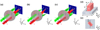 |
Fig. 1 Schematic diagram of the multiwavelength multifocal metalens and the unit cell. (a)–(c) Schematic diagram of LCP, RCP and LP light incidence at two wavelengths. λ1 =532 nm, λ2 =632 nm. (d), (e) Side view and top view of the unit cell. |
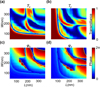 |
Fig. 2 The transmittance and phase delay as a function of the length and width of the nanofin at the wavelength of 632 nm. (a), (c) The transmittance Tx and phase delay φx of the linearly polarized light along the x direction. (b), (d) The transmittance Ty and phase delay φy of the linearly polarized light along the y direction. |
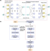 |
Fig. 3 Schematic diagram of the tandem network model and the design process. (a) The framework of the tandem network model. (b) The flow chart of the design process. |
2.2 The design of the tandem neural network model
The framework of the tandem network model, and the design process are shown in Figure 3. Among them,  and
and  are the target phase delays.
  ,
,  ,
,  , and
, and  are the target responses obtained after preprocessing the target phase delays. L and W are the structural parameters corresponding to the length and width of the unit cell.
  ,
,  ,
,  , and
, and  are the predicted responses obtained by the forward network based on the input L and W,
 and
and  are the predicted phase delays obtained after recovering the predicted responses. As shown in Figure 3a, the TNN consists of two parts: one is the forward network, which aims to predict the responses corresponding to the structural parameters, and the other one is the inverse network, aiming to design the structural parameters, based on the input responses and the predicted responses of the forward network. The inverse network avoids direct comparison of structural parameters, effectively overcoming the challenge of structural non-uniqueness in inverse scattering problems of the electromagnetic wave [38]. Compared to other inverse design algorithms, TNN has lower computational resource requirements and can establish relatively stable bidirectional mappings. However, it may fall into local optimum and the training effectiveness depends on high-quality data.
After preliminary testing, the number of nodes per layer in the forward network is set to 100, 250, 300, 250, and 100, respectively, and the Tanh function is selected as the nonlinear activation function in the output layer to ensure that the output values are limited to -1 to 1, while the number of nodes per layer in the inverse network is also set to 100, 250, 300, 250, and 100, respectively,and the output layer adopts the Softplus function, ensuring that the output is always greater than 0, thereby ensuring the rationality of structural parameters. At this time, the more reliable results can be obtained. The weight initialization adopts a normal distribution with the mean of 0 and the standard deviation of 0.1, ensuring that the initial value of the weight is within a reasonable range, avoiding gradient explosion or vanishing problems in back propagation, and helping to maintain the stability of the gradient. The random initialization of the normal distribution can also avoid different neurons learning the same features, ensuring that each neuron learns different features in the early stages of training. The bias initialization uses a constant of 0 to avoid introducing unnecessary bias in the early stages of network training, simplify the initial state of the network, and ensure that the output in the early stages of training is not affected by bias interference. What’s more, the batchsize is selected to 20, improving the model's generalization ability, while ensuring a higher update frequency and saving training time.
The Adaptive Moment Estimation (Adam) optimizer is selected as the optimizer with the defeat learing rate of 0.001, and the activation function takes Leaky Rectified Linear Unit (ReLU) function with the negative slope α = 0.1, solving the dead neuron problem of ReLU function that neurons fail to learn after entering the negative interval [39]. The activation function is expressed as:
 (1)
(1)
The purpose of neural network training is to make the predicted values as close as possible to the true values. The loss function takes the predicted and true values of all samples in the neural network as inputs, and outputs a scalar that reflects the overall difference between the predicted and true values. This scalar is called the loss. Loss is an overall metric for measuring the inaccuracy of neural network predictions on the entire dataset. Typically, minimizing loss is used as the objective in training to optimize parameters and improve prediction performance. The Huber loss function, which is also called SmoothL1 loss function, is chose as the loss function, and can be expressed as:
 (2)
(2)
where n is the number of samples, Yi represents the real values, and  denotes the predicted values, δ>0 (δ takes 0.1 after preliminary testing in this paper) is a scale parameter used to balance losses. The Huber loss function is not particularly sensitive to outliers and can adapt flexibly to the characteristics of different datasets [40]. When the predicted value is close to the real value, the effect is similar to the mean square error (MSE), and the gradient gradually decreases, ensuring that the model obtains the global optimal solution more accurately and has strong smoothness. When the predicted value is far from the real value, the effect is similar to the mean absolute error (MAE), maintaining a certain sensitivity and approximating the gradient to δ, ensuring that the model updates parameters at a faster rate, and preventing overfitting.
Figure 3b indicates the flow chart of the design process. The 10000 data pairs of the length and width are randomly generated by Matlab and stimulated by the finite-difference time-domain (FDTD) method to achieve the abundant phase data as the datasets, of which 80% are training sets, 15% are validation sets, and 5% are test sets. During the preprocessing process, the data pairs of the length and width vary as the ratio of the length and width to period, thereby accelerating the training rate. Through the trigonometric relation, the phase values are projected onto the unit circle with the center at the origin to transform phases into continuous x-y pairs, avoiding the influence of phase reference range (-π to π, or 0 to 2π), and fulfilling the normalization processing, to improve the prediction performance of the network [41].
During the training process, the max epoch is set to 500, and the patience, which can trigger early stopping, is adopted to prevent overfitting, and saving the training time. When the patience is too small, the network may fall into local minima without sufficient optimization, resulting in underfitting. When the patience is too large or removed, the network will continue to train for a long time, but the performance will no longer improve, wasting computing resources. After testing, when the patience is 20, the network can achieve relatively reliable results, so this paper chooses the patience value of 20.
The forward network is firstly trained, enabling it to form the mapping from the parameters to the responses, and then the weights and bias are fixed, assisting the training of the inverse network. Then, the inverse network is trained to minimize the difference between the input responses of the inverse network, and the predicted responses of the forward network corresponding to the output parameters of the inverse network. The loss function of the inverse network can be expressed as:
 (3)
(3)
Where Rreal is the real responses obtained through simulation, and Rpred is the predicted responses obtained from the forward network.
The performance of the TNN with the dataset at the wavelength of 632 nm is shown in Figure 4. Figure 4a shows the training loss and validation loss of the forward network. The best epoch is 168, and the best loss is 0.002053, taking about 2.31 minutes. Figure 4b depicts the testing effect of 500 test samples of the forward network. The average loss is 0.002101, close to the best loss, and the number of discrete spots is less, which indicates that the training of the forward network has obtained a relatively reliable result. Figure 4c shows the training loss and validation loss of the inverse network. The best epoch is 93, and the best loss is 0.002859, taking about 2.14 minutes. Figure 4d depicts the testing effect of 500 test samples of the inverse network, and the average loss is 0.003239, exceeding slightly the best loss. The training process for wavelengths’ simulations from 532 to 682 nm runs for a short time from 109 to 162 s, which is comparatively shorter than the GAN [42] and topology optimization [43], revealing the advantages of low computational resource requirements, hence less calculation time cost, while keeps high stability with TNN training. Although the number of discrete spots increases, and some values exceed the expected range of 0.1 to 0.9, the values remain within a reasonable range greater than 0 and less than 1. This is partly due the errors between the network training results and the actual results, and partly due to the non uniqueness of the unit cell that meets the design requirements of  at the same time.
What’s more, due to the number of training epochs actually running, the overall curve is non smooth. At the same time, because the training effect of inverse network depends on the prediction results of the forward network, the error of the forward network will be transferred to the inverse network. The inverse design involves a larger solution space, and there may be multiple local optimal solutions, resulting in more unstable training process. Therefore, the loss value is more significant, and the error is higher than that of the forward network. In addition, although the network performs well on the whole, in some specific samples, the predicted value may deviate greatly from the true value due to the fact that the parameter adjustment is still not fine enough and the randomness in the training process. When generating training data, the simulation may also introduce some numerical errors, which will be learned by the neural network during the training process, resulting in a large deviation between the predicted value and the real value of some samples. Some samples in the test set may have special characteristics, such as extreme phase distribution, but the frequency of occurrence in the training set is low, resulting in poor performance of the network in processing these samples. Finally, although Huber loss function has certain robustness to outliers, when the deviation is large, it will still cause the loss value to increase significantly. After the training of TNN, the design of the structure of the metalens can be started.
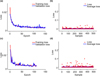 |
Fig. 4 Performance of the TNN. (a) Training loss and validation loss of the forward network. (b) Testing effect of the forward network. (c) Training loss and validation loss of the inverse network. (d) Testing effect of the inverse network. |
2.3 The principle and method of the phase modulation
In order to realize the multifocal metalens, a principle of composite phase modulation, which combines the manipulation of the propagation and PB (Pancharatnam-Berry) phases, is considered, so as to simultaneously and independently control RCP and LCP light, and realize the conversion between LCP and RCP light [44]. On the one hand, the control of the light field can be independently dependent on the polarization or spin state of the incident light by using the PB phase [45]. On the other hand, the propagation phase is related to the wavelength of the incident light and the refractive index of the material, and is independent of polarization or spin state. Therefore the phase is usually modulated by the differential proportions of two or more dielectrics (one of the dielectrics has a high refractive index) in the unit cell through the adjustment of the geometric size of the subwavelength structure [46].
Suppose the surface of the metalens is x-y plane, the vertical direction is z axis, and the center point is (0,0,0). Considering the focal length f and the corresponding position (xf, yf, zf) as the reference, the phase (φ) distribution at any position (x,y,0) can be obtained by
 (4)
(4)
where λ is the wavelength. The required phase distribution of the target focal position can be calculated through equation (4). When the orientation of the nanofin is rotated at the angle θ, the PB phase change is ±2θ for LCP and RCP light, respectively [47]. Considering the propagation phase (φPro), the PB phase (φPB), the required phase for LCP (φL) light and the required phase for RCP (φR) light [48]:
 (5)
(5)
Therefore, φPro and θ can be expressed as:
 (6)
(6)
Equation (6) shows that φPro and θ, can be determined by calculating the φL and φR. Considering the phase delay (φx and φy) of the nanofin for polarized light along the x and y axes, the phase should be satisfied [49]:
 (7)
(7)
Therefore, appropriate φPro can be obtained by:
 (8)
(8)
Equation (7) shows that the required geometric parameters, corresponding to φPro, can be obtained by calculating φx and φy of the nanofin along the x and y direction to realize the inverse design of metalens for different targets such as focusing and multi-focal imaging.
3 Result and discussion
3.1 Inverse design of the single-focus and bifocal metalenses
After the TNN is trained, in order to verity the performance of the proposed design, the single-focus metalens is chosen as the first design target. The single-focus metalens, as a relatively basic type of metalenses, can rely solely on the manipulation of the propagation phase, without changing the rotation angle of the nanofins based on the manipulation of PB phase, to test the the effectiveness of the parameters obtained by the trained network in practical applications. The designed metalens has the diameter of 11.2 μm and works at the wavelength of 632 nm.
Figures 5a and 5b depict the target and predicted phase distribution with the target focal length of 9 μm at 632 nm. The predicted phase distribution has generally approached the target distribution, but some regions are slightly different due to the errors in the prediction of the network. Through the numerical calculation of the prediction phase and target phase, the error is controlled below 3%, which indicates that there is a certain error in the prediction process of the network, and this error will have a certain impact on the accuracy of the subsequent simulation results. It can be seen that the current network design still has a large optimization space in terms of accuracy and robustness, and its performance can be further improved by improving the network structure and optimizing the training strategy in the future.
Figures 5c and 5d show the simulation results. Figure 5c shows that the intensity distribution in the x-z plane, the beam achieves an effective focal length near 9 μm, and the calculated simulated focal length height is 8.75 μm, with an error of about 2.7% from the target focal length. In addition, Figure 5d shows that strong focusing is achieved in the x-y plane at this height, forming a focusing spot, which indicates that the effect of crosstalk of the metalens is not significant. Full width at half maximum (FWHM) is usually used for analysis when evaluating the performance of metalens. FWHM refers to the wavelength difference where the intensity is half of the maximum peak value, reflecting the resolution and stability of the metlalens. At the height of the simulated focal length, the electric field intensity reaches the peak at the focus along the x and y directions, showing Gaussian distribution characteristics. After calculation, the FWHMs are 0.654 and 0.582 μm respectively. In addition to the neural network prediction error, the failure to fully consider the transmissivity of the unit cell and the refractive index of the material also have a certain impact on the imaging effect. Nevertheless, the experimental results verify the effectiveness of TNN in the transmission phase design, and provide a basis for further optimization design.
In order to realize the design of multiwavelength multifocus metalens, the wavelengths and the periods are changed to test the effect. The network is trained with the dataset of 532 nm wavelength and 350 nm period. As shown in Figures 6a and 6c, the simulated focal length height is 8.8 μm, the error is less than 2.3%, and the FWHMs along the x and y direction are 0.654 and 0.588 μm, respectively. However, due to the change of the period, the metalens does not match the focal length of the original target, causing certain impact. At the same time, it is necessary to frequently change the period and the focal length of the target to deal with different wavelengths, which causes some problems in the design of multiwavelength metalens. Therefore, the metalens with the same period (400 nm) as the original design is designed. Results as shown in Figure 6b and Figure 6d, the simulation focal length height is 9.4 μm, the error is controlled below 4.5%, and the FWHMs along the x and y directions are 0.57 μm and 0.546 μm respectively. Although the error is larger than the result at 350 nm, it is within the acceptable range, and the crosstalk is relatively optimized. The results show that in the same period, the design of different wavelengths has certain error changes, but within an acceptable range.
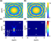 |
Fig. 5 The results of the designed single-focus metalens with the target focal length of 9 μm at the wavelength of 632 nm. (a) The target phase distribution calculated by the formula. (b) The predicted phase calculated by the TNN. (c),(d) The simulated electric field intensity distribution in the x-z, x-y plane with the simulated focal length of 8.75 μm. |
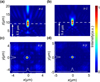 |
Fig. 6 The results of the single-focus metalens at the wavelength of 532 nm with different periods (a), (c) The intensity distribution in the x-z plane and x-y plane at 350 nm, and the simulated focal length is 8.8 μm (d) The intensity distribution in the x-z plane and x-y plane at 400 nm, and the simulated focal length is 9.4 μm. |
3.2 Inverse design of the bifocal metalens
Taking the design of the bifocal metalens as the example to test the capability of the designed structure generated by TNN in composite phase modulation to independently control LCP and RCP light. The designed metalens is able to convert the incident LCP light into RCP light, and focus at one point (2 μm, 0, 8 μm), while also converting the incident RCP light into LCP light, and focusing at the other point (–2 μm, 0, 8 μm). When the LP light is perpendicularly incident, the metalens can divide the LCP and RCP components, and focus at the corresponding positions, forming the bifocal image.
The simulation results are shown in Figure 7. When LCP or RCP light is incident, only a single focused spot is formed at the corresponding position, and the crosstalk effect is not significant. When LP light is incident, although the crosstalk in the middle of the x-z plane increases due to the existence of error and the superposition of LCP and RCP components, it is still within the controllable range and does not affect the imaging effect. As shown in Figure 7f, two symmetrical focused spots are formed in the x-y plane at the height of 8 μm. At the same time, the intensity distribution and FWHMs along the x direction at the origin of the simulation results are measured. When LCP light is incident, the light is focused on the right peak, while when RCP light is incident, it is focused on the left peak. When LP light is incident, the light focuses on the left and right wave peaks at the same time. In three cases, the peak to FWHM is 0.6 μm. The results show that the metalens can effectively divide LP light into LCP and RCP light components. It is verified that the structure can realize the independent control of LCP and RCP light on demand.
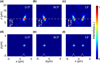 |
Fig. 7 The simulated results of the designed bifocal metalens. (a)-(f) The electric field intensity distribution in the x-z, x-y plane with the focal length of 8 μm of LCP, RCP, LP light incidence. |
3.3 Inverse design of the multiwavelength mulifocal metalens
On this basis, the multiwavelength multifocal metalens can be designed based on the TNN. The assumed dual-wavelength metalens is designed to work at two wavelengths (532 and 632 nm). At the wavelength of 532 nm, the phase of Si nanofin also covers 0 to 2π, and there is a certain difference in imaging effect compared to at a wavelength of 632 nm. The metalens with the diameter of 22.4 μm is divided into four regions. The lower left half circle is R1, the lower right half circle is R2, the upper left half circle is region R3 and the upper right half circle is R4. Meanwhile, each region can recognize the corresponding wavelength, and realize bifocal imaging independently. What’s more, the positions of the bifocal spots are symmetric in the region R1 and R3, while asymmetric in the region R2 and R4. The expected focus distribution is shown in Table 1.
The simulation results of the dual wavelength multifocal metalens operating at 532 and 632 nm under different incident light conditions are shown in Figure 8, in which R1 and R4 are designed for 532 nm, while R2 and R3 are designed for 632 nm. Figures 8a–8c show the intensity distribution of the metalens in the x-y plane at the wavelength of 532 nm. When LCP light or RCP light is incident, the light can focus on a corresponding spot in R1 and R4, while no significant spots are formed in the remaining regions. When LP light is incident, two corresponding spots are formed in both R1 and R4. Figures 8d–8f show the case when the wavelength is 632 nm. In contrast to 532 nm, significant light spots can be formed at the corresponding positions in R2 and R3, while no significant light spots can be formed in R1 and R4. Meanwhile, the period of 400 nm is mainly designed for 632 nm, and the training effect of the two groups of networks is different, some structures of 532 nm are relatively seriously affected by crosstalk.
The intensity distribution of each region of the metalens is further analyzed, and the results are shown in Figure 9. When the wavelength is 532 nm, the intensity distributions in R1 and R4 are concentrated in the corresponding positions, and the degree of oscillation is relatively stable compared with that in the other two regions. The locations with relative intensity higher than 0.5 also meet the design requirements. Similarly, when the wavelength is 632 nm, the intensity distributions are concentrated in the corresponding positions in R2 and R3, and the overall electric field intensity is more stable than that in 532 nm, indicating that the metalens is indeed subject to a certain amount of crosstalk interference at 532 nm. At the same time, due to the modulation of the propagation phase by changing the sizes of the unit cells, the electric field intensity is relatively high in the designed positions, so that the weak foci appear, but the relative intensity does not exceed 0.5, which is within the acceptable range. The results show that the metalens can achieve ideal focusing effect in most cases, and the interaction between different regions is not significant, leading to independent imaging between regions. What’s more, the results verify the feasibility of TNN in the design of complex functions of metalens.
In order to verify the sensitivity of the metalens to wavelengths, the focusing effects of LP light incidence at 10 wavelengths, including 500, 532, 550, 582, 600, 632, 650, 682, 700 and 732 nm, are simulated and analyzed, and the results are shown in Figure 10. Between 500 and 550 nm, relatively significant spots can be formed in R1 and R4, but the focusing effect at 500 or 550 nm is less significant than that at 532 nm, due to the influence of the crosstalk. At 582 nm, the effect of the crosstalk is salient, and there is no significant focusing effect. At 600 nm, as the crosstalk effect weakens, the focusing effect is enhanced in R2 and R3, while weak foci remain in R1 and R4. Between 632 and 732 nm, there is significant focusing effect in R2 and R3. The crosstalk effect is serious again at 732 nm, and the light spots are relatively loose. The focusing effects at 600, 682 and 700 nm are also affected by crosstalk, and inferior to those at 632 and 650 nm.
As shown in Figure 11, the relative intensity above 0.5 in R1 is mainly between the wavelength of 500 and 582 nm. Combined with Figures 10g and 10j, the focusing effect is weakened and the slight position shifts occur at 582 nm, and the occurrence of relative intensity above 0.5 at 732 nm is mainly due to weak focusing caused by crosstalk. The relative intensity above 0.5 in R2 is mainly between 582 and 732 nm. The relative intensity near the lower focal point is above 0.5 at 500 nm and 550 nm, and below 0.5 at 532 nm. It may be due to crosstalk, as well as the weakening of the focusing effect in R1 and R3. At the same time, the phase of the structure at different wavelengths is relatively close, resulting in weak focusing. The relative intensity above 0.5 in R3 is mainly between 600 and 732 nm. The relative intensity above 0.5 at the focus at 582 nm is due to the weakening of the focusing effect and the influence of crosstalk. The relative intensity above 0.5 in R4 is mainly between 500 and 582 nm. At 600 nm, due to the enhanced focusing effect in R2 and R3, the effect of the crosstalk is reduced, and the phase requirement at this point is close at different wavelengths. Therefore, the relative intensity at this point is still above 0.5, but it has weakened relative to 582 nm.
The expected focus distribution of the multiwavelength multifocal metalens.
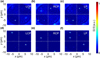 |
Fig. 8 The simulation results of the dual-wavelength metalens under different conditions of the incident light. (a)–(c) The electric field intensity distribution in the x-y plane of LCP, RCP, LP light incidence at 532 nm. (d)–(f) The electric field intensity distribution in the x-y plane of LCP, RCP, LP light incidence at 632 nm. |
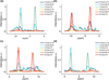 |
Fig. 9 The simulation results of the electric field intensity distribution along the x or y direction of each region of the dual-wavelength metalens. (a) The intensity distribution along the x direction in R1. (b) The intensity distribution along the y direction in R2. (c) The intensity distribution along the y direction in R3. (d) The intensity distribution along the x direction in R4. |
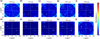 |
Fig. 10 The electric field intensity distribution in the x-y plane of dual-wavelength metalens of LP light incidence at different wavelengths. (a) 500 nm (b) 532 nm (c) 550 nm (d) 582 nm (e) 600 nm (f) 632 nm (g) 650 nm (h) 682 nm (i) 700 nm (j) 732 nm. |
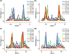 |
Fig. 11 The simulation results of the electric field intensity distribution along the x or y direction of each region at different wavelengths (a) The intensity distribution along the x direction in R1. (b) The intensity distribution along the y direction in R2. (c) The intensity distribution along the y direction in R3. (d) The intensity distribution along the x direction in R4. |
 |
Fig. 12 The electric field intensity distribution in the x-y plane of the multiwavelength metalens of LP light incidence at different wavelengths. (a) 500 nm (b) 532 nm (c) 550 nm (d) 582 nm (e) 600 nm (f) 632 nm (g) 650 nm (h) 682 nm (i) 700 nm (j) 732 nm. |
3.4 Further research of the metalens
Furthermore, the wavelength of the metalens is extended to four wavelengths, including 532, 582, 632, and 682 nm. R2 is designed for 582 nm, while R4 is designed for 682 nm. The results are shown in Figure 12. At 500 nm, the formation of the spots can be observed in R1. At 532 nm, the significant spots are formed in R1, and the crosstalk in other regions is improved. At 550 nm, the focusing effect in R1 is weakened, and the focusing effect begins to form in R2. At 582 nm, the significant spots are formed in R2, and the spots in R1 disappeaR. At 600 nm, the focusing effect in R2 weakened, the focus effect begins to form in R3, and weak foci appear in R1 and R4. At 632 nm, the significant spots are formed in R3, and the focusing effect in R2 continue to weaken, leaving a weak focus. At 650 nm, the focus effect in R2 continue to weaken, and the spots begin to form in R4. At 682 nm, the significant spots are formed in R4, the spot disappears in R2 and the focusing effect weakens in R3. At 700 nm, the focusing effect continue to weaken in R3 and R4. At 732 nm, the spots in R3 and the left focus in R4 weaken to the weak foci.
The electric field intensity distribution in each region is further analyzed, and the results are shown in Figure 13. At 500 nm, the crosstalk effect is serious, the intensity changes violently, and there is no obvious focusing effect, so the situation, that the relative intensity is above 0.5 occurs in every regions. The relative intensity above 0.5 in R1 is mainly between 532 and 550 nm. The relative intensity above in R2 is mainly between 550 and 600 nm It can be observed that the focusing effect is significantly weakened at 550 nm and 600 nm. The relative intensity above 0.5 in R3 is mainly between 600 and 682 nm. The relative intensity above 0.5 in R4 is mainly between 650 and 732 nm, and the focusing effect of the left focus is weaker than that of the right focus at 732 nm.
Through in-depth analysis of the above-mentioned metalens design, it can be seen that the constructed tandem neural network can effectively realize the forward prediction of the corresponding phase of the metalens structure and the inverse design of the structure corresponding to the phase distribution, so as to meet the design requirements of single-focus and even multiwavelength multifocal metalens. Therefore, it can be inferred that the tandem neural network can show significant potential in the inverse design of metalens with more complex functions and applications. However, it can also be seen from the predicted phase distribution and simulation results that the current design still has room for optimization due to errors and deficiencies caused by accuracy, crosstalk produced by FDTD simulation and small residual errors in neural network training. In addition, the unit cell selects a relatively simple square cylinder structure, and the parameters involved in the network design are only the lengths and widths. The more complex structure and more design parameters will still pose challenges to the tandem neural network. In the design process, factors such as transmittance and absorption loss are not fully considered, which may lead to the performance degradation of the metalens. With the continuous progress and optimization of neural network algorithm and simulation technology, it can be expected that the deepening and expansion of the intelligent design of metalens will significantly improve the design performance. In terms of network design, physical information neural network (PNN) with physical constraints is introduced, PINN) [50], the physical model-based neural network (pmnn) [51] and other networks closer to the physical laws are added to the network training to ensure that the generated structure not only meets the data-driven optimization objectives, but also meets the basic physical laws, so as to reduce the dependence on a large number of training data and improve the physical rationality of the design. With the continuous development and integration of technology, the inverse design method based on deep learning will show wider application potential in the design of metalens, and promote the development of optical devices to higher performance and more complex functions.
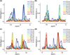 |
Fig. 13 The simulation results of the electric field intensity distribution along the x or y direction of each region of the multiwavelength metalens at different wavelengths. (a) The intensity distribution along the x direction in R1. (b) The intensity distribution along the y direction in R2. (c) The intensity distribution along the y direction in R3. (d) The intensity distribution along the x direction in R4. |
4 Conclusions
In summary, the inverse design method of the multiwavelength multifocal metalens base on the TNN is proposed. The TNN neural network effectively resolves the non-uniqueness problem in electromagnetic inverse scattering, and demonstrates strong stability as well as reliable convergence while does not depend on perfectly curated training data, which enables efficient training on large-scale datasets. The inverse design method avoids the traditional complex and time-consuming process, providing a fast customization path for the design of metalenses. The designed single-focus metalens with the design error controlled below 2.8% indicates that this method can customize the focal length and the simulation results are close to the target. The designed bifocal metalens realizes the independently control of RCP and LCP light. Finally, the designed multiwavelength multifocal metalens can recognize different wavelengths, and realize the independent imaging among the regions, forming bifocal spots at corresponding positions. By changing the wavelengths, the sensitivity of the metalens to wavelengths is demonstrated, indicating that it can be used for wavelength detection. The designed metalenses have potential application value and further development prospects in the fields of optical communication, imaging, and detection.
Funding
The Science and Technology Commission of Shanghai Municipality (Grant No. 21DZ1100500), the Shanghai Municipal Science and Technology Major Project, the Shanghai Frontiers Science Center Program (2021-2025 No. 20), the National Key Research and Development Program of China (Grant No. 711 2021YFB2802000), and the National Natural Science Foundation of China (Grant No. 62205209).
Conflicts of interest
The authors declare no conflicts of interest.
Data availability statement
Data underlying the results presented in this paper are not publicly available at this time but may be obtained from the authors upon reasonable request.
Author contribution statement
Conceptualization, supervision and Funding acquisition: Mingyu Sun. Investigation and writing: Yilun Song.Data collection and data curation: Bowei Wu.
References
- S. Li, C. Hsu, Thickness bound for nonlocal wide-field-of-view metalenses, Light Sci. Appl. 11, 338 (2022) [Google Scholar]
- H. Tie, L. Wen, H. Li et al., Aberration-corrected hybrid metalens for longwave infrared thermal imaging, Nanophotonics 13, 3059 (2024) [Google Scholar]
- B. Wang, Y. Xu, Z. Wu et al., All-dielectric metasurface-based color filter in CMOS image sensor, Optics Commun. 540, 129485 (2023) [Google Scholar]
- C. Shen, R. Xu, J. Sun et al., Metasurface-Based Holographic Display With All-Dielectric Meta-Axilens., IEEE Photon. J. 13, 4600105 (2021) [Google Scholar]
- L. Rui, H. Yuan, Z. Zhong et al., Non-volatile and switchable encrypted metasurface for simultaneous nanoprinting and holography, Optical Mater. 151, 115306 (2024) [Google Scholar]
- X. Chen, Y. Zhang, L. Huang et al., Ultrathin Metasurface Laser Beam Shaper, Adv. Opt. Mater. 2, 978 (2014) [Google Scholar]
- Z. Zhuang, R. Chen, Z. Fan et al., High focusing efficiency in subdiffraction focusing metalens, Nanophotonics 8, 1279 (2019) [Google Scholar]
- Y. Liu, J. Lin, Y. Lin, Reconfigurable metalens with dual-linear-focus phase distribution, Optics Laser Technol. 164, 109526 (2023) [Google Scholar]
- I.A. Atalay, Y.A. Yilmaz, F.C. Savas et al., A Broad-Band Achromatic Polarization-Insensitive In-Plane Lens with High Focusing Efficiency, ACS Photon. 8, 2481 (2021) [Google Scholar]
- Y. Chu, X. Xiao, X. Ye et al., Design of achromatic hybrid metalens with secondary spectrum correction, Opt. Express 31, 21399 (2023) [Google Scholar]
- G. Go, C.H. Park, K.Y. Woo et al., Scannable Dual-Focus Metalens with Hybrid Phase, Nano Lett. 23, 3152 (2023) [Google Scholar]
- A. Amin, D. Ghafar, N.M. Mohammad et al., Switchable visible and near-infrared light bifocal lens based on hybrid graphene-metasurface structures, Diamond & Related Mater. 143, 110945 (2024) [Google Scholar]
- Y. Hu, Y. Wang, Q. Xu et al., Design of monofocal and bifocal lenses by new method and their application in high-gain lens antenna based on chiral metamaterial, IET Microwaves, Antennas & Propagation 13, 2272 (2019) [Google Scholar]
- J. Zhang, H. Liang, Y. Long et al., Metalenses with Polarization‐Insensitive Adaptive Nano‐Antennas, Laser & Photon. Rev. 16, 9 (2022) [Google Scholar]
- L. Chen, Z. Shao, J. Liu et al., Multi-wavelength achromatic bifocal metalenses with controllable polarization-dependent functions for switchable focusing intensity, J. Phys. D: Appl. Phys. 55, 115102 (2022) [Google Scholar]
- T. Sun, J. Hu, X.J. Zhu et al., Broadband Single-Chip Full Stokes Polarization-Spectral Imaging Based on All-Dielectric Spatial Multiplexing Metalens, Laser Photon. Rev. 16, 2100650 (2022) [Google Scholar]
- Z. Li, J. Xu, L. Zhang et al., Inverse Design of Dual-Band Optically Transparent Metasurface Absorbers with Neural-Adjoint Method, Annal. Phys. 535, 6 (2023) [Google Scholar]
- E. Adibnia, B. Mansouri, A. Mohammad et al., A deep learning method for empirical spectral prediction and inverse design of all-optical nonlinear plasmonic ring resonator switches, Sci. Rep. 14, 5787 (2024) [Google Scholar]
- Y. Yin, Q. Jiang, H. Wang et al., Multi-dimensional Multiplexed Metasurface Holography by Inverse Design, Adv. Mater. 36, e2312303 (2024) [Google Scholar]
- D. Zhang, Z. Liu, X. Yang et al., Inverse Design of Multifunctional Metasurface Based on Multipole Decomposition and the Adjoint Method, ACS Photon. 9, 3899 (2022) [Google Scholar]
- S. Xiao, F. Zhao, D. Wang et al., Inverse design of a near-infrared metalens with an extended depth of focus based on double-process genetic algorithm optimization, Opt. Express 31, 8668 (2023) [Google Scholar]
- H. Chung, O.D. Miller, High-NA achromatic metalenses by inverse design, Opt. Express 28, 6945 (2020) [Google Scholar]
- T. Ye, D. Wu, Q. Wu et al., Realization of inversely designed metagrating for highly efficient large angle beam deflection, Opt. Express 30, 7566 (2022) [Google Scholar]
- L. Gu, Y. He, H. Liu et al., Metasurface meta-atoms design based on DNN and LightGBM algorithms, Optical Mater. 136, 113471 (2023) [Google Scholar]
- C.Y. Xi, H.L. Fen, Inverse design of reflective metasurface antennas using deep learning from small‐scale statistically random pico‐cells, Microwave Optical Technol. Lett. 66, e34068 (2024) [Google Scholar]
- R.W. Peter, A. Arnaud, G. Christian et al., Deep learning in nano-photonics: inverse design and beyond, Photon. Res. 9, 584 (2021) [Google Scholar]
- S. An, B. Zhen, H. Tang et al., Multifunctional Metasurface Design with a Generative Adversarial Network, Adv. Optical Mater. 9, 2001433 (2021) [Google Scholar]
- K. Qu, K. Chen, Q. Hu et al., Deep-learning-assisted inverse design of dual-spin/frequency metasurface for quad-channel off-axis vortices multiplexing, Adv. Photon. Nexus 2, 016010 (2023) [Google Scholar]
- Y. Yin, Q. Jiang, H. Wang et al., Multi-Dimensional Multiplexed Metasurface Holography by Inverse Design, Adv. Mater. 36, e2312303 (2024) [Google Scholar]
- Y. Al-Alem, S. M. Sifat, Y.M.M. Antar et al., Low-Cost Circularly Polarized Millimeter-Wave Antenna using 3D Additive Manufacturing Dielectric Polarizer, 2021 IEEE International Symposium on Antennas and Propagation and USNC-URSI Radio Science Meeting (APS/URSI), Singapore, 2021, pp. 1425–1426 [Google Scholar]
- S. Wang, K. Chen, S. Dong et al., Tunable topological polaritons by dispersion tailoring of an active metasurface, Adv. Photon. 6, 046005 (2024) [Google Scholar]
- Y. Chen et al., Inverse design of ultracompact multi-focal optical devices by diffractive neural networks, Opt. Lett. 47, 2842 (2022) [Google Scholar]
- F. Wang, X. Shu, Design of a bifocal metalens with tunable intensity based on deep-learning-forward genetic algorithm, J. Phys. D: Appl. Phys. 56, 095101 (2023) [Google Scholar]
- X. He, X. Cui, C.T. Chan, Constrained tandem neural network assisted inverse design of metasurfaces for microwave absorption, Opt. Express 31, 40969 (2023) [Google Scholar]
- S. Wang, Y. He, H. Zhu et al., An Efficient Design Method for a Metasurface Polarizer with High Transmittance and Extinction Ratio, Photonics 11, 53 (2024) [Google Scholar]
- P. Xu, J. Lou, C. Li et al., Inverse design of a metasurface based on a deep tandem neural network, J. Opt. Soc. Am. B 41, A1 (2024) [Google Scholar]
- X. Li, S. Chen, D. Wang et al., Transmissive mid-infrared achromatic bifocal metalens with polarization sensitivity, Opt. Express 29, 17173 (2021) [Google Scholar]
- D Liu, Y Tan, E Khoram et al., Training Deep Neural Networks for the Inverse Design of Nanophotonic Structures, ACS Photon. 5, 1365 (2018) [Google Scholar]
- J. Xu, Z. Li, B. Du et al., Reluplex made more practical: Leaky ReLU, Proceedings - IEEE Symposium on Computers and Communications 2020 -July (2020) [Google Scholar]
- Y. Sun, X. Fang, Robust Calibration of Computer Models Based on Huber Loss, J. Syst. Sci.& Complexity 36, 1717 (2023) [Google Scholar]
- X. An, Y. Cao, Y. Wei et al., Broadband achromatic metalens design based on deep neural networks, Opt. Lett. 46, 3881 (2021) [Google Scholar]
- Zhaocheng LiuDayu ZhuSean P. Rodrigues et al., Generative Model for the Inverse Design of Metasurfaces, Nano Lett. 18, 6570 (2018) [Google Scholar]
- S. Stich, J. Mohajan, D. Ceglia et al., Inverse Design of an All-Dielectric Nonlinear Polaritonic Metasurface, ACS Nano 19, 17374 (2025) [Google Scholar]
- M.J.P. Balthasar, N.A. Rubin, R.C. Devlin et al., Metasurface Polarization Optics: Independent Phase Control of Arbitrary Orthogonal States of Polarization, Phys. Rev. Lett. 118, 113901 (2017) [Google Scholar]
- G. Biener, A. Niv, V. Kleiner et al., Formation of helical beams by use of Pancharatnam-Berry phase optical elements, Opt. Lett. 27, 1875 (2002) [Google Scholar]
- P.R. West, J.L. Stewart, A.V. Kildishev et al., All-dielectric subwavelength metasurface focusing lens, Opt. Express 22, 26212 (2014) [Google Scholar]
- Z. Jiang, M. Chao, Q. Liu et al., High-efficiency spin-selected multi-foci terahertz metalens, Optics Lasers Eng. 174, 107816 (2024) [Google Scholar]
- W. Wang, Q. Yang, S. He et al., Multiplexed multi-focal and multi-dimensional SHE (spin Hall effect) metalens, Opt. Express 29, 43270 (2021) [Google Scholar]
- S. Li, X. Li, G. Wang et al., Multidimensional Manipulation of Photonic Spin Hall Effect with a Single‐Layer Dielectric Metasurface, Adv. Opt. Mater. 7, 1801365 (2019) [Google Scholar]
- K. Alexander et al., Magnetostatics and micromagnetics with physics informed neural networks, J. Magnetism Magnetic Mater. 548, 168951 (2022) [Google Scholar]
- J. He et al., Physics-model-based neural networks for inverse design of binary phase planar diffractive lenses, Opt. Lett. 48, 1474 (2023) [Google Scholar]
Cite this article as: Yilun Song, Bowei Wu, Mingyu Sun, Inverse design of multiwavelength multifocal metalens based on the tandem neural networks, EPJ Appl. Metamat. 13, 13 (2026), https://doi.org/10.1051/epjam/2025017
All Tables
All Figures
|
Fig. 1 Schematic diagram of the multiwavelength multifocal metalens and the unit cell. (a)–(c) Schematic diagram of LCP, RCP and LP light incidence at two wavelengths. λ1 =532 nm, λ2 =632 nm. (d), (e) Side view and top view of the unit cell. |
| In the text | |
|
Fig. 2 The transmittance and phase delay as a function of the length and width of the nanofin at the wavelength of 632 nm. (a), (c) The transmittance Tx and phase delay φx of the linearly polarized light along the x direction. (b), (d) The transmittance Ty and phase delay φy of the linearly polarized light along the y direction. |
| In the text | |
|
Fig. 3 Schematic diagram of the tandem network model and the design process. (a) The framework of the tandem network model. (b) The flow chart of the design process. |
| In the text | |
|
Fig. 4 Performance of the TNN. (a) Training loss and validation loss of the forward network. (b) Testing effect of the forward network. (c) Training loss and validation loss of the inverse network. (d) Testing effect of the inverse network. |
| In the text | |
|
Fig. 5 The results of the designed single-focus metalens with the target focal length of 9 μm at the wavelength of 632 nm. (a) The target phase distribution calculated by the formula. (b) The predicted phase calculated by the TNN. (c),(d) The simulated electric field intensity distribution in the x-z, x-y plane with the simulated focal length of 8.75 μm. |
| In the text | |
|
Fig. 6 The results of the single-focus metalens at the wavelength of 532 nm with different periods (a), (c) The intensity distribution in the x-z plane and x-y plane at 350 nm, and the simulated focal length is 8.8 μm (d) The intensity distribution in the x-z plane and x-y plane at 400 nm, and the simulated focal length is 9.4 μm. |
| In the text | |
|
Fig. 7 The simulated results of the designed bifocal metalens. (a)-(f) The electric field intensity distribution in the x-z, x-y plane with the focal length of 8 μm of LCP, RCP, LP light incidence. |
| In the text | |
|
Fig. 8 The simulation results of the dual-wavelength metalens under different conditions of the incident light. (a)–(c) The electric field intensity distribution in the x-y plane of LCP, RCP, LP light incidence at 532 nm. (d)–(f) The electric field intensity distribution in the x-y plane of LCP, RCP, LP light incidence at 632 nm. |
| In the text | |
|
Fig. 9 The simulation results of the electric field intensity distribution along the x or y direction of each region of the dual-wavelength metalens. (a) The intensity distribution along the x direction in R1. (b) The intensity distribution along the y direction in R2. (c) The intensity distribution along the y direction in R3. (d) The intensity distribution along the x direction in R4. |
| In the text | |
|
Fig. 10 The electric field intensity distribution in the x-y plane of dual-wavelength metalens of LP light incidence at different wavelengths. (a) 500 nm (b) 532 nm (c) 550 nm (d) 582 nm (e) 600 nm (f) 632 nm (g) 650 nm (h) 682 nm (i) 700 nm (j) 732 nm. |
| In the text | |
|
Fig. 11 The simulation results of the electric field intensity distribution along the x or y direction of each region at different wavelengths (a) The intensity distribution along the x direction in R1. (b) The intensity distribution along the y direction in R2. (c) The intensity distribution along the y direction in R3. (d) The intensity distribution along the x direction in R4. |
| In the text | |
|
Fig. 12 The electric field intensity distribution in the x-y plane of the multiwavelength metalens of LP light incidence at different wavelengths. (a) 500 nm (b) 532 nm (c) 550 nm (d) 582 nm (e) 600 nm (f) 632 nm (g) 650 nm (h) 682 nm (i) 700 nm (j) 732 nm. |
| In the text | |
|
Fig. 13 The simulation results of the electric field intensity distribution along the x or y direction of each region of the multiwavelength metalens at different wavelengths. (a) The intensity distribution along the x direction in R1. (b) The intensity distribution along the y direction in R2. (c) The intensity distribution along the y direction in R3. (d) The intensity distribution along the x direction in R4. |
| In the text | |
Current usage metrics show cumulative count of Article Views (full-text article views including HTML views, PDF and ePub downloads, according to the available data) and Abstracts Views on Vision4Press platform.
Data correspond to usage on the plateform after 2015. The current usage metrics is available 48-96 hours after online publication and is updated daily on week days.
Initial download of the metrics may take a while.