


Fig. 2
Download original image
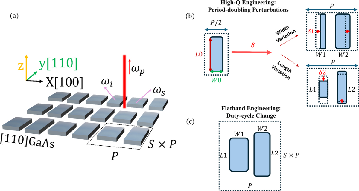
(a) Geometrical layout of the proposed flatband resonant metasurface. Periodic GaAs (made from [110] cut GaAs) metasurface with a period of P in x-direction and S × P in y-direction and thickness of 300 nm. S represents a non-zero scaling factor, which gives a different pitch in x- and y- directions. The substrate SiO2 is not shown for simplicity. (b) & (c) shows the geometry engineering introduced to respectively generate high-Q and flatband features.
Current usage metrics show cumulative count of Article Views (full-text article views including HTML views, PDF and ePub downloads, according to the available data) and Abstracts Views on Vision4Press platform.
Data correspond to usage on the plateform after 2015. The current usage metrics is available 48-96 hours after online publication and is updated daily on week days.
Initial download of the metrics may take a while.